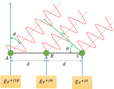
The array is a periodic structure in space with elements placed at equidistant. d/λ acts as the frequency term and λ/d as the time period. The incremental phase shift between adjacent elements is (2π/λ)×d×[sin(θ)-sin(θ0)]. d is the inter-element distance in unit of λ, θ-any position during the scanning of the array and θ0 – the angular direction set for the array to transmit/receive with the main lobe having the maximum gain.
For the ensuing discussion here, let us assume that no preferred direction θ0 is set and the array is free to scan from its broadside (θ=0°) to the limits of scan ± 90° or u=± 1. The inter-element phase shift now is (2π/λ) × d × u, where u = sin θ, and the magnitude of phase shift attains a maximum at |u|=1.
The below Fig.1 traces the phase function for various values of d, as it is increased from 0.25 λ to 2 λ.


Two apparent factors emerge from this plot: As d is increased between the elements, the rate of phase change is higher and the range between u=-1 and u=1 is also increased. The field is sampled (for its amplitude and phase) at each element and the sampling is repeated at the spatial interval of d. Up to a distance of d≤ λ/2, the maximum phase difference between adjacent elements is ≤ π for |u|=1, and increases beyond this limit for d> λ/2. This means that samples between elements are taken at least once, within a phase difference of π, as long as d≤ λ/2. The visible phase region for a scan limit from u=-1 to u= 1, is 2π when d≤ λ/2 condition exists; and taking at least one sample per π radians satisfies the Nyquist criterion (π radians being the Nyquist space). This condition no longer exists when the inter-element distance is increased beyond λ/2.
For example, if d= λ, the maximum phase difference between adjacent elements is 2π for |u|=1. But the sampling once between adjacent elements now spans a phase range of 2π, resulting in a clear case of under sampling in the spatial domain. The situation becomes even more critical when d is further increased. As observed earlier, the rate of phase difference between elements and the total range for (u=-1 to u=1), climb up to such levels, much poorer sampling rates happen among the elements. This results in increasing spatial aliasing, akin to what one experiences in the case of under sampled signals in the frequency domain.
Such spatial aliasing result in the occurrence of extra peaks (with near similar values of the main beam) and thus create disruptions in the antenna pattern. They result in giving wrong directional readings as well as sharing the power and distributing it in unwanted zones of the antenna array pattern. Such events are named as the presence of grating lobes.
Examination of the occurrence and placement of grating lobes:
As seen in the earlier section, the resultant field of a linear array of N elements is given by:


[ E= the field intensity at each element (transmit/receive) and δ=(2π/λ)×d×(u-u0) ]
Grating lobes were discussed so far only with respect to the increase of inter-element distance > λ/2. But there are other contributing factors too.
- The inter-element phase δ has three variables such as λ, d and u0. For narrow band systems, the dispersion in the operating wavelength is small and may be ignored; but in wideband and ultra-wideband systems it is a factor to reckon with. In such cases, both phase shift and time delay circuits will have to be employed.
- The effect of increasing d >λ/2 has already been discussed for the occurrence of spatial aliasing.
- The setting of u0 has limitations on the available scan width to avoid the grating lobe formation. This will be taken up a little later.
For attaining the peak value for the antenna main lobe, it is clear that sin(δ) = 0, making the expression using the following L’Hospital’s rule↗.


Hence, sin (δ/2) = sin [(π/λ)×d×(u-u0)] = 0 =sin (±mπ), where m=0,1,2,3,………
So,


or,


In the above equations, parameters u and u0 can have both positive and negative values, but their maximum magnitude is 1 = (|sin(±π/2)|, which is the visible region in sin(θ) space).
Hence,


Let us now examine as to how this important relationship helps in determining the presence of grating lobes and their angular locations.
- Case (1): d=λ/2; u= u0±m(λ/d) = u0 ±m×2; u0 is chosen in all these cases to be zero for this study, hence it could be ignored and the equation can be simplified to u= ±m (λ/d), with the condition |±m (λ/d) | max =1.
- For m=0, u= 0, indicating the broadside beam at θ=0°.
- For m=1, u=±2 and this not in the visible region.
- For still higher values of m, the results are not going yield any beam in the visible region. Hence the conclusion is that there is one unique peak and no other lobes of near equal magnitude in the visible range. Hence no grating lobe. This will be the case for all d ≤ λ/2.
- Case(2): d=λ; u= ±m (λ/d)= ±m;
- For m=0, u=0; beam at θ=0°, as before.
- For m=1, u=±1, grating lobes at u= sin (π/2) and u=sin (-π/2)
- For m =2, u=±2, (not valid for visible range) and this is true for all values of m≥2
- In conclusion we see, that increase in the inter-distance element d =λ, produces two grating lobes at the edge of the scan range.
- Case (3): d=1.5 λ; u= ±m (λ/d) = ± 0.66m.
- For m=0, u=0; beam at θ=0°, as before
- For m=1, u=± 0.66, grating lobes at θ = sin-1 (± 0.66) = ± 41.3°
- For m =2, u=±1.34, (not in the visible range; true for all values of m ≥ 2)
- Case(4): d=2λ; u= ±m (λ/d)= ± 0.5 m;
- For m=0, u=0, beam at θ=0°, as before.
- For m=1, u= ± 0.5, so two grating lobes at θ= sin -1 (± 0.5) = ± 30°.
- For m=2, u= ± 1, indicating another pair of grating lobes at θ=±90°.
- For m=3, u= ± 1.5 (not valid for visible range). This is the result for all values of m≥ 3. The final tally in this case is the presence of 4 grating lobes along with the main beam
- Summary
| d (with u0 = 0) | M (Spatial Harmonics) | Grating Lobes |
|---|---|---|
| ≤ λ/2 | m=0 | Nil (Main beam only) |
| λ | m=0 m=1 | Nil(Main beam only); Present @ u=± 1 |
| 1.5λ | m=0 m=1 | Nil(Main beam only); Present @ u=± 0.66 |
| 2λ | m=0 m=1 m=2 | Nil (Main beam only); Present @u=±0.5 Present @ u=± 1 |
Simulation and results
A simulation run with N=100 in the MATLAB application environment produced the following plot (Fig.2). The plot line in blue indicates the array pattern with d=λ/2 and the line plotted with red color is for the case of d=λ. The third plot in green is for d=1.5 λ. Conclusion arrived in the calculation above are duly verified by this simulation.


The result of a simulation, done to validate the finding in case 4, is given below (Fig.3). The case for d= λ/2 is again taken as reference and blue color line plot indicates its array pattern. The plot with d=2 λ, shows the main beam along with a pair of grating lobes at u=±0.5. Another pair appears u=± 1 (at the edges of the scan) as predicted by the calculation above.


It will be observed that up to d ≤ λ/2, the higher values of spatial harmonic multiplier (m> 0) is not used, since the value of λ/d ≥ 2. It is only the higher values of d/ λ which become smaller fractions on inverting to λ/d, need this harmonic multiplier to satisfy the relationship and answer to the allowable magnitude of |u|max=1. Hence the presence of grating lobes for larger values of d> λ/2.
Designing an array for maximum performance
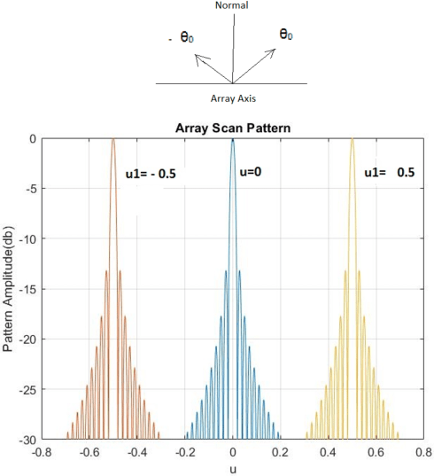
Having completed this trial, let us now examine the consequence of designing an array for maximum performance at a directed angle of u0=0.5.
The conditional statement at equation (4) is modified to include the requirement of u0 to be set for a value of 0.5:


- Case 1: Checking the case for λ/d=2 to set the reference: u= -1 ≤ [0.5 ±m (2)] ≤ 1
- For m=0, u=0.5, giving the required main beam at the set value of 0.5.
- No other grating lobe with higher harmonic number (m>0) is possible here.
- So up to d /λ ≤ 0.5, no grating lobes occur as seen earlier.
- Case 2:For d= λ, u= -1 ≤ [0.5 ±m×(1)] ≤ 1
- For m=0 : u=0.5 again;
- For m=1, u=0.5± 1 which yields a grating lobe at u=-0.5; Values higher than m≥2, do not reveal any presence of grating lobe in the visible region.
- Case 3: For d=1.5 λ, u= -1 ≤ [0.5 ±m×(0.66)] ≤ 1;
- For m=0 : u=0.5;
- For m=1, u= ±0.66, show a pair of grating lobe at θ= ±41.3°.
- For m=2, u=0.5-1.32=-0.82 yield a grating lobe at θ= -55.1°.
- Values higher than m≥3, do not reveal any presence of grating lobe in the visible region.
- Case 4: For d=2 λ, u= -1 ≤ [0.5 ±m×(0.5)] ≤ 1;
- For m =0: u=0.5;
- For m =1, u= {0, 1}, shows a pair of grating lobes at θ=0° and 90°
- For m=2, u=0.5-1.00=-0.5 yield a grating lobe at θ= -30°.
- For m=3, u=0.5-1.5 =-1 show a grating lobe at θ= -90°.
- Once again, values higher than m≥3, do not reveal any presence of grating lobe in the visible region.
- Simulation and Results
(i) Occurrence of Grating Lobes: when d= λ ,(with d= λ/2 as reference)


The above plot (Fig.4) shows the simulation results for the two cases of d=λ/2 and λ. The validation can be checked through two methods: By plotting the phase data against u, we are able to identify the zeros of the function at which points zero- crossings occur. It will also identify the multiple points where it occurs for d > λ/2. By co-locating the array pattern below, one can easily correlate position of zeros with that of the locations of the grating lobes.
(ii) Similarly, Fig.5 below represents the simulation results and validation for the case d=1.5λ and 2λ.


Limits of Scan imposed by Grating Lobes
Revisiting the relationship for the array to perform in the visible region of u=sin(θ) space, we have


For the safe scanning of the array without the presence of grating lobes, the above condition must be sustained. Let us see how this limit plays out for various values of d (the inter-element spacing), subjected to the limit |u|max=1 for visual range.
It is obvious that as the inter-element space d increases from λ/2, the limits on the permissible scan range gets reduced, if one were to avoid the presence of grating lobes in the operating region. Table 2 compares the allowable scan limits for various values of the inter-element spacing with the constraint that |u|max=1.
| d/λ | Electronic Scanning Limits (|u0| =0 ) | Electronic Scanning Limits ( |u0|>0) |
|---|---|---|
| 1/2 | -1 ≤ u ≤ 1 (Full visual range) | -1 ± |u0 | ≤ u ≤ 1 ± |u0| |
| 1 | -0.5 ≤ u ≤ 0.5 | 0.5 ± |u0 | ≤ u ≤ 0.5 ± |u0 | |
| 1.5 | -0.33 ≤ u ≤ 0.33 | -0.33 ± |u0 | ≤ u ≤ 0.33 ± |u0 | |
| 2 | -0.25 ≤ u ≤ 0.25 | -0.25 ± |u0 | ≤ u ≤ 0.25 ± |u0 | |
Simulation results to confirm these limits are presented below for the case of a linear array of 100 elements, with d=1.5, with two conditions: |u0|= 0 and 0.2.
Case 1: With the condition u0=0, the allowable scan limits are u= ± 0.33;
In the first simulation run, the array scan was arranged to be within allowable limits of u=±0.33 with u0 set to zero. As predicted by the calculation, there is no grating lobe under this situation (Fig. 6). If now, the scan is increased to the full range of visible region (u= ± 1), grating lobes @ u=±o.66, as predicted, appear on either side of the main coverage (Fig. 7) :
Absence of Grating Lobes when scan is within u= ± 0.33; (N=100, d=1.5λ, u0=0)


Occurrence of Grating lobes when scan range exceeds limit of u= ± 0.33


Case 2 : (i) In this simulation, ‘u0‘ is set to a value 0f 0.2 and the simulation repeated as done for the case 1. In the following instance, the permissible range for u is -0.33+0.2 ≤ u ≤ 0.33+0.2; Hence no grating lobe is seen within this region [-0.13≤ u ≤ 0.53].(Fig. 8, below).The top plot gives the locations of the zeros of the phase function. Correspondence of the location of the peak at u=0.2 can be verified with both the plots.
(ii) In the case of the array being scanned to the limits -1≤ u ≤ 1, the appearance of the grating lobes and their angular positions are validated with the calculations shown earlier : (lower plot of Fig.8)


Note: To make the scanning range flexible in the simulation, a window function was generated to move along the ‘u’ axis with variable range limits. The following Fig.9, illustrates the results obtained.
A phase function window was generated for a scan range of u= ± 0.33 and ± 0.7. (Blue and Red lines respectively). In the first case the array exhibits no grating lobe as per the calculation. The second case is beyond the permissible scan range and hence shows the presence of grating lobes. Such windowing function helps to evaluate different scan ranges quickly for a designer.


In conclusion, it is stressed that electronic scanning is not without limitation (true for any technology), but it is amenable to system optimization with many of the parameters under the designer’s dynamic control.
Continue reading on Array pattern multiplication …
Note: There is a rating embedded within this post, please visit this post to rate it.Articles in this series
- Phased Array Antenna – an introduction
- Electronic Scanning Arrays
- Grating lobes in electronic scanning (this article)
- Array pattern multiplication