Key focus: Array pattern multiplication: total radiation pattern of N identical antennas is product of single-antenna radiation vector and array factor.
An antenna array is a collection of numerous linked antenna elements that operate together to broadcast or receive radio waves as if they were a single antenna. Phased array antennas are used to focus the radiated power towards a particular direction. The angular pattern of the phased array depends on the number of antenna elements, their geometrical arrangement in the array, and relative amplitudes and phases of the array elements.
Phased array antennas can be used to steer the radiated beam towards a particular direction by adjusting the relative phases of the array elements.
The basic property of antenna arrays is the translational phase-shift.
Time-shift property of Fourier transform
Let’s focus for a moment on the time-shifting property of Fourier transform. The time–shifting property implies that a shift in time corresponds to a phase rotation in the frequency domain.
Now, let’s turn our attention to antenna elements translated/shift in space. Figure 1 depicts a single antenna element having current density J(r) placed at the origin is moved in space to a new location that is l0 distant from the original position. The current density of the antenna element at the new position l0 is given by
\[J_{l_0}(r) = J(r – l_0) \quad \quad (2)\]
Figure 1: Current density of antenna element shifted in space
Therefore, from equations (2) and (3), the radiation vector of the antenna element space-shifted to new position l0 is given by the space shift property (similar to time-shift property of Fourier transform in equation (1))
\[\begin{aligned} \mathbf{F}_{l_0} \left(\mathbf{k} \right) &=\int_V J_{l_0}(r)e^{j \mathbf{k} \cdot r } d^3 r \\
&= \int_V J(r-l_0)e^{j \mathbf{k} \cdot r } d^3 r \\ &= \int_V J(r)e^{j \mathbf{k} \cdot (r+l_0) } d^3 r \\
&= e^{j \mathbf{k} l_0}\int_V J(r)e^{j \mathbf{k} \cdot r } d^3 r \\ &= e^{j \mathbf{k} l_0} \mathbf{F} \left(\mathbf{k} \right) \end{aligned}
\\
\Rightarrow \boxed{ \mathbf{F}_{l_0} \left(\mathbf{k} \right) = e^{j \mathbf{k} l_0} \mathbf{F}\left(\mathbf{k} \right) }
\quad \quad (4) \]
Note: The sign of exponential in the Fourier transform does not matter (it just indicates phase rotation in opposite direction), as long as the same convention is used throughout the analysis.
From equation (4), we can conclude that the relative location of the antenna elements with regard to one another causes relative phase changes in the radiation vectors, which can then contribute constructively in certain directions or destructively in others.
Array factor and array pattern multiplication
Figure 2 depicts a more generic case of identical antenna elements placed in three dimensional space at various radial distances l0, l1, l2, l3, … and the antenna feed coefficients respectively are a0, a1, a2, a3,…
Figure 2: Current densities of antenna elements shifted in space – contributors to array factor of phased array antenna
The current densities of the individual antenna elements are
The quantity A(k) is called array factor which incorporates the relative translational phase shifts and the relative feed coefficients of the array elements.
The array pattern multiplication property states that the total radiation pattern of an antenna array constructed with N identical antennas is the product of radiation vector of a single individual antenna element (also called as element factor) and the array factor.
Effect of array factor on power gain and radiation intensity
Let U(θ,ɸ) and G(θ,ɸ) denote the radiation intensity and the power gain patterns of an antenna element. The total radiation intensity and the power gain of an antenna array, constructed with such identical antenna elements, will be modified by the array factor as follows.
The role of array factor is very similar to that of the transfer function of an linear time invariant system. Recall that if a wide sense stationary process x(t) is input to the LTI system defined by the transfer function H(f), then the power spectral density of the output is given by
\[S_y(f) = \mid H(f) \mid ^2 S_x(f)\]
Illustration using a linear array of half-wave dipole antennas
Linear antennas are electrically thin antennas whose conductor diameter is very small compared to the wavelength of the radiation λ.
A linear antenna oriented along the z-axis has radiation vector (field) whose components are along the directions of the radial distance and the polar angle. That is, the radiation intensity U(θ,ɸ) and the power gain G(θ,ɸ) depend only on the polar angle θ. In other words, the radiation intensity and the power gain are omnidirectional (independent of azimuthal angle ɸ).
Figure 3, illustrates an antenna array with linear half-wave dipoles placed on the x-axis at equidistant from each other.
Figure 3: A linear antenna array with half-wave dipole elements
We are interested in the power gain pattern G(θ,ɸ) of the antenna array shown in Figure 3.
The normalized power gain pattern of an individual antenna element (half-wave dipole) is given by
Figure 4 illustrates equation (15) – the effect of array factor on normalized power gain of an array of half-wave dipole antennas. The plot is generated for separation distance between antenna elements l=λ and the feed coefficients for the antenna elements a = [1, -1, 1].
Check out my Google colab for the python code. The results are given below.
Figure 4: Illustrating the effect of array pattern multiplication on normalized power gain of antenna array
If the element pattern of an array is very broad (as in an Omni directional antenna element) the pattern of the array is mostly the Array Factor since it is more directional. However, if the element pattern has some distinctive features by employing specific illumination function, then the composite radiation pattern is obtained by the principal of pattern multiplication. If Farrayis the Fourier transform of the array field and Felement is the Fourier transform of the element field, the combined pattern is given by the pattern multiplication
Composite antenna pattern = Farray × Felement
Example:
Uniformly illuminated array produces a first sidelobe level of -13.5 dB [=20×log10 (field amplitude)]. Due to the vast difference in levels between major and minor lobes, logarithmic (dB) scale is preferred in such measurements to provide the required dynamic range. This illumination function produces a better aperture efficiency (gain), sharper beamwidth but at the cost of near sidelobes getting elevated.
Figure 1: Radiation pattern with uniform aperture illumination
2. The cosine aperture distribution on a pedestal attempts to deal with a maximized gain along with control on the sidelobe levels. The accompanying figure below is the array pattern with illumination function of the type f(x) =0.9×cos(x) +0.1, where x refers to the linear position of the element.
Figure 2: Radiation pattern with cosine aperture illumination
Instead of tapering the edge illumination to zero, the cosine function sits on a pedestal to provide a constant illumination, but at a lower percentage level, at the peripheral geometry of the radiating element. The main beam is broadened but the first sidelobes are at -23.5dB level, an order of improvement on the -13.5 dB level of the previous case.
Several sophisticated illumination functions are available to the designer now to optimize array design.
Concluding remarks
It should be stressed that a Phased Array produces huge opportunity for designers to exploit its dynamic properties; but at the same time, it challenges us with system engineering and integration complexity, maintainability and finally in the cost factor. In an evolving era of technology, limitations in engineering and operation, would always witness a better tomorrow, provided the basic scientific validation and sustainability are present in all of the newer innovations.
Rate this post: Note: There is a rating embedded within this post, please visit this post to rate it.
Note: There is a rating embedded within this post, please visit this post to rate it.
The array is a periodic structure in space with elements placed at equidistant. d/λ acts as the frequency term and λ/d as the time period. The incremental phase shift between adjacent elements is (2π/λ)×d×[sin(θ)-sin(θ0)]. d is the inter-element distance in unit of λ, θ-any position during the scanning of the array and θ0 – the angular direction set for the array to transmit/receive with the main lobe having the maximum gain.
For the ensuing discussion here, let us assume that no preferred direction θ0 is set and the array is free to scan from its broadside (θ=0°) to the limits of scan ± 90° or u=± 1. The inter-element phase shift now is (2π/λ) × d× u, where u = sin θ, and the magnitude of phase shift attains a maximum at |u|=1.
The below Fig.1 traces the phase function for various values of d, as it is increased from 0.25 λ to 2 λ.
Fig. 1 Phase range Vs. d/λ
Two apparent factors emerge from this plot: As d is increased between the elements, the rate of phase change is higher and the range between u=-1 and u=1 is also increased. The field is sampled (for its amplitude and phase) at each element and the sampling is repeated at the spatial interval of d. Up to a distance of d≤ λ/2, the maximum phase difference between adjacent elements is ≤ π for |u|=1, and increases beyond this limit for d> λ/2. This means that samples between elements are taken at least once, within a phase difference of π, as long as d≤ λ/2. The visible phase region for a scan limit from u=-1 to u= 1, is 2π when d≤ λ/2 condition exists; and taking at least one sample per π radians satisfies the Nyquist criterion (π radians being the Nyquist space). This condition no longer exists when the inter-element distance is increased beyond λ/2.
For example, if d= λ, the maximum phase difference between adjacent elements is 2π for |u|=1. But the sampling once between adjacent elements now spans a phase range of 2π, resulting in a clear case of under sampling in the spatial domain. The situation becomes even more critical when d is further increased. As observed earlier, the rate of phase difference between elements and the total range for (u=-1 to u=1), climb up to such levels, much poorer sampling rates happen among the elements. This results in increasing spatial aliasing, akin to what one experiences in the case of under sampled signals in the frequency domain.
Such spatial aliasing result in the occurrence of extra peaks (with near similar values of the main beam) and thus create disruptions in the antenna pattern. They result in giving wrong directional readings as well as sharing the power and distributing it in unwanted zones of the antenna array pattern. Such events are named as the presence of grating lobes.
Examination of the occurrence and placement of grating lobes:
As seen in the earlier section, the resultant field of a linear array of N elements is given by:
[ E= the field intensity at each element (transmit/receive) and δ=(2π/λ)×d×(u-u0) ]
Grating lobes were discussed so far only with respect to the increase of inter-element distance > λ/2. But there are other contributing factors too.
The inter-element phase δ has three variables such as λ, d and u0. For narrow band systems, the dispersion in the operating wavelength is small and may be ignored; but in wideband and ultra-wideband systems it is a factor to reckon with. In such cases, both phase shift and time delay circuits will have to be employed.
The effect of increasing d>λ/2 has already been discussed for the occurrence of spatial aliasing.
The setting of u0has limitations on the available scan width to avoid the grating lobe formation. This will be taken up a little later.
For attaining the peak value for the antenna main lobe, it is clear that sin(δ) = 0, making the expression using the following L’Hospital’s rule↗.
Hence, sin (δ/2) = sin [(π/λ)×d×(u-u0)] = 0 =sin (±mπ), where m=0,1,2,3,………
So,
or,
In the above equations, parameters u and u0 can have both positive and negative values, but their maximum magnitude is 1 = (|sin(±π/2)|, which is the visible region in sin(θ) space).
Hence,
Let us now examine as to how this important relationship helps in determining the presence of grating lobes and their angular locations.
Case (1):d=λ/2; u= u0±m(λ/d)= u0 ±m×2; u0 is chosen in all these cases to be zero for this study, hence it could be ignored and the equation can be simplified to u= ±m (λ/d), with the condition |±m (λ/d) | max =1.
For m=0, u= 0, indicating the broadside beam at θ=0°.
For m=1, u=±2 and this not in the visible region.
For still higher values of m, the results are not going yield any beam in the visible region. Hence the conclusion is that there is one unique peak and no other lobes of near equal magnitude in the visible range. Hence no grating lobe. This will be the case for all d ≤ λ/2.
Case(2):d=λ; u= ±m (λ/d)= ±m;
For m=0, u=0; beam at θ=0°, as before.
For m=1, u=±1, grating lobes at u= sin (π/2) and u=sin (-π/2)
For m =2, u=±2, (not valid for visible range) and this is true for all values of m≥2
In conclusion we see, that increase in the inter-distance element d =λ, produces two grating lobes at the edge of the scan range.
Case (3):d=1.5 λ; u= ±m (λ/d) = ± 0.66m.
For m=0, u=0; beam at θ=0°, as before
For m=1, u=± 0.66, grating lobes at θ = sin-1 (± 0.66) = ± 41.3°
For m =2, u=±1.34, (not in the visible range; true for all values of m ≥ 2)
Case(4): d=2λ; u= ±m (λ/d)= ± 0.5 m;
For m=0, u=0, beam at θ=0°, as before.
For m=1, u= ± 0.5, so two grating lobes at θ= sin -1 (± 0.5) = ± 30°.
For m=2, u= ± 1, indicating another pair of grating lobes at θ=±90°.
For m=3, u= ± 1.5 (not valid for visible range). This is the result for all values of m≥ 3. The final tally in this case is the presence of 4 grating lobes along with the main beam
Table No.1: Inter-Element Spacing Vs. Presence of Grating Lobes
Simulation and results
A simulation run with N=100 in the MATLAB application environment produced the following plot (Fig.2). The plot line in blue indicates the array pattern with d=λ/2 and the line plotted with red color is for the case of d=λ. The third plot in green is for d=1.5 λ. Conclusion arrived in the calculation above are duly verified by this simulation.
Fig.2Array Pattern for increasing d/λ
The result of a simulation, done to validate the finding in case 4, is given below (Fig.3). The case for d= λ/2 is again taken as reference and blue color line plot indicates its array pattern. The plot with d=2 λ, shows the main beam along with a pair of grating lobes at u=±0.5. Another pair appears u=± 1 (at the edges of the scan) as predicted by the calculation above.
Fig.3: Antenna Pattern for d=λ/2 and 2λ
It will be observed that up to d ≤ λ/2, the higher values of spatial harmonic multiplier (m> 0) is not used, since the value of λ/d≥ 2. It is only the higher values of d/ λ which become smaller fractions on inverting to λ/d, need this harmonic multiplier to satisfy the relationship and answer to the allowable magnitude of |u|max=1. Hence the presence of grating lobes for larger values of d> λ/2.
Designing an array for maximum performance
Having completed this trial, let us now examine the consequence of designing an array for maximum performance at a directed angle of u0=0.5.
The conditional statement at equation (4) is modified to include the requirement of u0 to be set for a value of 0.5:
Case 1: Checking the case for λ/d=2 to set the reference: u= -1 ≤ [0.5 ±m (2)] ≤ 1
For m=0, u=0.5, giving the required main beam at the set value of 0.5.
No other grating lobe with higher harmonic number (m>0) is possible here.
So up to d /λ ≤ 0.5, no grating lobes occur as seen earlier.
Case 2:For d= λ, u= -1 ≤ [0.5 ±m×(1)] ≤ 1
For m=0 : u=0.5 again;
For m=1, u=0.5± 1 which yields a grating lobe at u=-0.5; Values higher than m≥2, do not reveal any presence of grating lobe in the visible region.
Case 3: For d=1.5 λ, u= -1 ≤ [0.5 ±m×(0.66)] ≤ 1;
For m=0 : u=0.5;
For m=1, u= ±0.66, show a pair of grating lobe at θ= ±41.3°.
For m=2, u=0.5-1.32=-0.82 yield a grating lobe at θ= -55.1°.
Values higher than m≥3, do not reveal any presence of grating lobe in the visible region.
Case 4: For d=2 λ, u= -1 ≤ [0.5 ±m×(0.5)] ≤ 1;
For m =0: u=0.5;
For m =1, u= {0, 1}, shows a pair of grating lobes at θ=0° and 90°
For m=2, u=0.5-1.00=-0.5 yield a grating lobe at θ= -30°.
For m=3, u=0.5-1.5 =-1 show a grating lobe at θ= -90°.
Once again, values higher than m≥3, do not reveal any presence of grating lobe in the visible region.
Simulation and Results
(i) Occurrence of Grating Lobes: when d= λ ,(with d= λ/2 as reference)
Fig. 4Grating lobe for d=λ
The above plot (Fig.4) shows the simulation results for the two cases of d=λ/2 and λ. The validation can be checked through two methods: By plotting the phase data against u, we are able to identify the zeros of the function at which points zero- crossings occur. It will also identify the multiple points where it occurs for d > λ/2. By co-locating the array pattern below, one can easily correlate position of zeros with that of the locations of the grating lobes.
(ii) Similarly, Fig.5 below represents the simulation results and validation for the case d=1.5λ and 2λ.
Fig. 5: Grating lobes for d= 1.5λ & 2λ
Limits of Scan imposed by Grating Lobes
Revisiting the relationship for the array to perform in the visible region of u=sin(θ) space, we have
For the safe scanning of the array without the presence of grating lobes, the above condition must be sustained. Let us see how this limit plays out for various values of d (the inter-element spacing), subjected to the limit |u|max=1 for visual range.
It is obvious that as the inter-element space d increases from λ/2, the limits on the permissible scan range gets reduced, if one were to avoid the presence of grating lobes in the operating region. Table 2 compares the allowable scan limits for various values of the inter-element spacing with the constraint that |u|max=1.
d/λ
Electronic Scanning Limits (|u0| =0 )
Electronic Scanning Limits ( |u0|>0)
1/2
-1 ≤ u ≤ 1 (Full visual range)
-1 ± |u0 | ≤ u ≤ 1 ± |u0|
1
-0.5 ≤ u ≤ 0.5
0.5 ± |u0 | ≤ u ≤ 0.5 ± |u0 |
1.5
-0.33 ≤ u ≤ 0.33
-0.33 ± |u0 | ≤ u ≤ 0.33 ± |u0 |
2
-0.25 ≤ u ≤ 0.25
-0.25 ± |u0 | ≤ u ≤ 0.25 ± |u0 |
Table 2 : d/λ Vs. Electronic Scan Limits
Simulation results to confirm these limits are presented below for the case of a linear array of 100 elements, with d=1.5, with two conditions: |u0|= 0 and 0.2.
Case 1: With the condition u0=0, the allowable scan limits are u= ± 0.33;
In the first simulation run, the array scan was arranged to be within allowable limits of u=±0.33 with u0 set to zero. As predicted by the calculation, there is no grating lobe under this situation (Fig. 6). If now, the scan is increased to the full range of visible region (u= ± 1), grating lobes @ u=±o.66, as predicted, appear on either side of the main coverage (Fig. 7) :
Absence of Grating Lobes when scan is within u= ± 0.33; (N=100, d=1.5λ, u0=0)
Fig. 6: No grating lobe for scan range u = ± 0.33
Occurrence of Grating lobes when scan range exceeds limit of u= ± 0.33
Fig. 7 Occurrence of grating lobes when scan range extends to u=± 1
Case 2 : (i) In this simulation, ‘u0‘ is set to a value 0f 0.2 and the simulation repeated as done for the case 1. In the following instance, the permissible range for u is -0.33+0.2 ≤ u ≤ 0.33+0.2; Hence no grating lobe is seen within this region [-0.13≤ u ≤ 0.53].(Fig. 8, below).The top plot gives the locations of the zeros of the phase function. Correspondence of the location of the peak at u=0.2 can be verified with both the plots.
(ii) In the case of the array being scanned to the limits -1≤ u ≤ 1, the appearance of the grating lobes and their angular positions are validated with the calculations shown earlier : (lower plot of Fig.8)
Fig. 8: Grating lobes : When Scan Range extends to u=± 1
Note: To make the scanning range flexible in the simulation, a window function was generated to move along the ‘u’ axis with variable range limits. The following Fig.9, illustrates the results obtained.
A phase function window was generated for a scan range of u= ± 0.33 and ± 0.7. (Blue and Red lines respectively). In the first case the array exhibits no grating lobe as per the calculation. The second case is beyond the permissible scan range and hence shows the presence of grating lobes. Such windowing function helps to evaluate different scan ranges quickly for a designer.
Fig. 9: Grating Lobes (by using window function for ‘u’)
In conclusion, it is stressed that electronic scanning is not without limitation (true for any technology), but it is amenable to system optimization with many of the parameters under the designer’s dynamic control.
This is considered to be the best feature of a phased array antenna. To be able to scan in a given space, without having to rotate the antenna is called inertia less scanning and serves many advantages, especially in field operations.
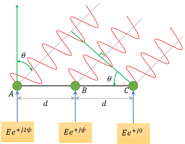
To illustrate the principle, let us take a simple three element linear array arranged with the following phase relationship due to its beam tilted towards an angle θ to receive signal, as shown below:
Figure 1: A simple three element linear array
The path difference between adjacent elements is= d sin (θ) and it progressively increases from right to left. So BB’= d sin (θ) whereas CC’= 2d sin (θ). If we assume that an incoming field with planar wavefront having equal amplitude and equiphase is across CC’, one can visualize the extra path that has to be traveled to reach element A and B, in comparison to the element C. Translating this into phase shift, we have a phase delay= φB = (2π/λ) d sin (θ) at element B, and φA= (2π/λ)(2d)sin(θ) at element A, all reckoned with element C as the point of phase reference. So in the final tally, the field captured along the three-element array comes out to be EResultant = E (1+e-jφ+ e-j2φ), where φ = (2π/λ) d sin(θ) and E is the field value of the incoming equiphase front. The magnitude of the resultant field can be simplified to E(1+2 cos (φ)). It is clear that the field captured by all elements adds up to 3E only when cos (φ) equals zero, which is the case when the antenna is looking at its perpendicular direction, called the broadside. But this is the initial position without scanning. The expression further shows that array gain falls as the angle of scan increases, theoretically falling to E at φ=± π/2. (A simple vector diagram will reveal that at this state, the field received by element A will oppose that of element C). This position also coincides with the limits of scan in the visible region corresponding to a scan limit of θ= ± 90°, for (d/λ) =1/2.
The above example forms the basis for exploring the method of electronic scanning, further.
If we need to receive a signal from an angle inclined from the bore-sight (θ=0°), then there is an inevitable phase shift (delay) to signal reaching the different elements. Hence the uniform phase front along the linear antenna array is no longer along its axis but lifted (refer line CC’) at an angle equal to the angle of scan, (θ in the above example). If we wish to bring back this tilted equiphase plane along the axis of the array, it is obvious each element should now have a phase shift of its own to counter the phase delay they suffered. The required phase shift would be equal in magnitude but in opposite direction.
Let the array be now modified with each element provided with a phase shifter individually. A phase shift + ψ is introduced in a progressive manner from left to right to compensate the phase delays produced earlier by the incoming signal.
Figure 2: Array elements with phase shifters
The modified array equation gives the resultant field = E (1+e-j(φ-ψ) + e-j2(φ-ψ))
Making (φ-ψ) = δ, the above reduces to Ee-j δ(e+jδ + 1 + e-jδ)= E e-j δ [1+2 cos (δ)], which attains maximum at δ =0, making φ=ψ. Remember that φ=(2π/λ) d sin (θ).
Suppose we want the beam to position at θ=30°, then ψ = (2π/λ) d sin (30°). If we need to scan to a direction θ=-30°, then ψ =- (2π/λ) d sin(30°), will be a lagging phase shift.
What essentially resulted was that the equiphase plane inclined at θ was brought back to the array surface by phase weighting (ψ) of the element as arranged in Figure 2. The phase weight is dependent on the angle chosen for the scan, once the designer has already selected the spacing among elements (d/λ). This phase weight will then have to continually track its value in sync with the position of the scan angle ‘θ ‘.
A general equation can now be attempted to describe the pattern of a linear array antenna with N elements:
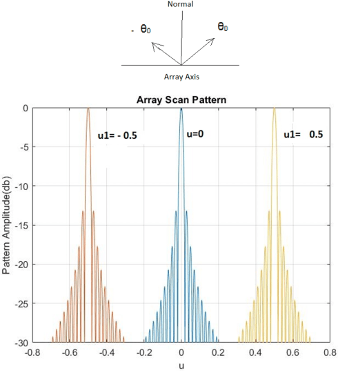
A simulation run with an array antenna is shown in Figure 1. A linear array of 100 elements was chosen (N=100), with the inter-distance between elements d=λ/2. The desired angle of scan was u1=sin(θ0) This was set for three values: u=0 (broadside), and at u1=± 0.5 (angle of ±30°).
Figure 3: Array scan pattern
It is true that the gain of the scanned patterns becomes a function of the scanned angle [Gθ = G cos(θ)]; this fact is not visible in this plot as each pattern is normalized with respect to its own peak.
Since the latter half of previous century, a class of antenna technology called the ‘Phased Arrays’ has witnessed phenomenal progress in design, engineering and applications. Concurrent progress in solid state material has enabled active antenna elements to be packed as arrays in many different geometries- linear, planar and conformal shapes. Though started as the solution for various taxing military needs, this technology has since entered many civilian domains, the space applications being one of the prominent usage in the present times.
Phased Array, which employs simpler elemental antennas to configure a complex system, has many interesting features and capabilities. The first one that appeals to a designer, is the ability to address the design problem by reaching at the elemental level for control. Theoretically, it is possible to control at each element, the amplitude and phase of the signal being fed. This gives rise to a dynamic control of antenna beam shape, electronic scanning, sidelobes and their placement-all leading to a variety of applications from the same system.
Though amplitude and phase control are possible at element level, it is generally seen that the designers use the amplitude control to set the illumination function of the elements and deal with the dynamic requirements by phase shifter switching. Presently, phase shifters are capable of being engineered in small form factor, incorporating the solid state source, the connecting geometry and the radiating element. Digital and modular technology make it feasible for mass production and for maintainability and reliability in severe environmental condition.
The phase shifters employed in such systems use solid state devices and electronically controlled ferrites for switching. They are typically controlled with 4 to 5 bits digital accuracy which give enough phase states to design for. The setting accuracy of a phase state has also considerably advanced in that a designer can plan for dynamic beam shaping with confidence. By dividing the entire R.F. source among many elements, the power management and heat dissipation of the system get distributed to manageable engineering practice. Hence such a level of sophistication on phase control has finally evolved an array system, justifiably called the ‘Phased Array Antenna’.
In the succeeding pages, effort has been made to describe what is the unique specialty of Phased Arrays- ‘the electronic steering’ –its value and also the limitations, so that a balanced view is derived. The idea is to employ simple examples to start with and build on this initial strength to move onto more intricate antenna functions. The emphasis will be on the design concepts and their practical utility. No deeper background in EM theory, RF-Microwave practices are required at present; but essential knowledge of antennas and their different operating frequency environments are already visible to everyone in today’s technology bound world.
It is presumed that readers are familiar with many of the antenna concepts and parameters, like antenna gain, beamwidth, sidelobes, field and power patterns, reciprocity in antenna for transmitting and receiving; and allied engineering mathematical concepts like Fourier Transform, geometric series and their summation, and the need for logarithmic compression in the plotting of antenna patterns. Such an initial preparation will help in assimilating the text and graphics which follow.
This website uses cookies to improve your experience while you navigate through the website. Out of these, the cookies that are categorized as necessary are stored on your browser as they are essential for the working of basic functionalities of the website. We also use third-party cookies that help us analyze and understand how you use this website. These cookies will be stored in your browser only with your consent. You also have the option to opt-out of these cookies. But opting out of some of these cookies may affect your browsing experience.
Necessary cookies are absolutely essential for the website to function properly. These cookies ensure basic functionalities and security features of the website, anonymously.
Cookie
Duration
Description
cookielawinfo-checbox-analytics
11 months
This cookie is set by GDPR Cookie Consent plugin. The cookie is used to store the user consent for the cookies in the category "Analytics".
cookielawinfo-checbox-analytics
11 months
This cookie is set by GDPR Cookie Consent plugin. The cookie is used to store the user consent for the cookies in the category "Analytics".
cookielawinfo-checbox-functional
11 months
The cookie is set by GDPR cookie consent to record the user consent for the cookies in the category "Functional".
cookielawinfo-checbox-functional
11 months
The cookie is set by GDPR cookie consent to record the user consent for the cookies in the category "Functional".
cookielawinfo-checbox-others
11 months
This cookie is set by GDPR Cookie Consent plugin. The cookie is used to store the user consent for the cookies in the category "Other.
cookielawinfo-checbox-others
11 months
This cookie is set by GDPR Cookie Consent plugin. The cookie is used to store the user consent for the cookies in the category "Other.
cookielawinfo-checkbox-necessary
11 months
This cookie is set by GDPR Cookie Consent plugin. The cookies is used to store the user consent for the cookies in the category "Necessary".
cookielawinfo-checkbox-performance
11 months
This cookie is set by GDPR Cookie Consent plugin. The cookie is used to store the user consent for the cookies in the category "Performance".
viewed_cookie_policy
11 months
The cookie is set by the GDPR Cookie Consent plugin and is used to store whether or not user has consented to the use of cookies. It does not store any personal data.
Functional cookies help to perform certain functionalities like sharing the content of the website on social media platforms, collect feedbacks, and other third-party features.
Performance cookies are used to understand and analyze the key performance indexes of the website which helps in delivering a better user experience for the visitors.
Analytical cookies are used to understand how visitors interact with the website. These cookies help provide information on metrics the number of visitors, bounce rate, traffic source, etc.